Table of Contents
555 timer circuits are good to learn after becoming familiar with the basic components.
There’s 3 basic 555 timer circuits that most text covers. I also like to add the inverter Schmitt trigger to the list.
- Bistable:
- Monostable:
- Astable:
- Inverter Schmitt Trigger (bonus):
Assorted integrated circuits (ICs) kit. Included is the NE555 timers and other commonly known ICs. I have previously covered some of the other ICs in YouTube videos. It is an Affiliate link ad that supports this channel.
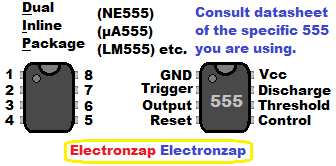
Integrated circuits are usually drawn in schematics as a square or rectangle with their part number in the middle. They also show connections to their various pin numbers in a way that makes the diagram look good.
- High output is when the output connects to the positive supply as best as that it can. Usually losing about 1.5V.
- Low output is when the output connects to the negative power supply (ground and 0V) as best that it can. the 555 does a pretty good job at connecting to ground.
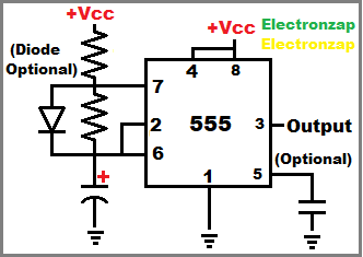
Basic 555 Bistable circuit:
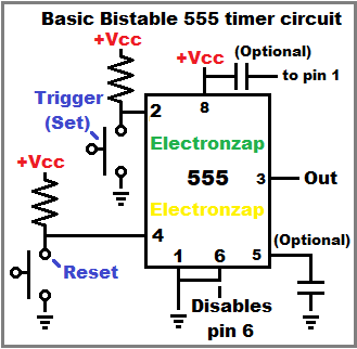
- Bistable: Two (bi) stable states. Output stays either high or low, until forced to change.
- Low signal to Trigger sets output high (as long as there is no low input to Reset pin). The output stays high, as long as there is no low signal to Reset pin.
- Low signal to Reset pin sets the output low and keeps it low until the Reset pin is set high and the Trigger gets a low input.
Low value capacitors connecting the 1 and 8 supply pins, and pin 5 to ground, help stabilize the voltages across them. A steady supply voltage is important as the internal circuitry responds to voltages in relationship to the supply voltage.
The 555 timer will often work OK without those capacitors.
Basic Monostable 555 circuit:
- Monostable: One (mono) stable state. Output stays low until triggered with a low signal. That sets the output high for a period of time, and then goes back low and stays there until triggered again.
- While output is low, pin 7 is also low (connected to ground within the IC), keeping the capacitor discharged to 0V.
- When output is high, due to a low input pulse at pin 2 (trigger), pin 7 basically turns off. No current flows through it. So, capacitor can start charging.
- When capacitor charges to 2/3 Vcc, output goes back to low, and capacitor instantly discharges through pin 7, which also goes low. Resistor and capacitor values determines the time that it takes for the capacitor to go from 0 volts, to two thirds of the supply voltage.
Light pulse sets off short active buzzer alarm using monostable mode 555 timer circuit
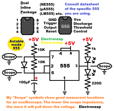
Basic Astable 555 Timer Circuit:
When power is first applied…
The 6 & 2 to ground capacitor charges through Vcc resistor and diode until it gets to 2/3 supply voltage (Vcc). During that time, output is high.
Capacitor hitting 2/3Vcc tells pin 6 to set the output low, and pin 7 goes low as well. They both connect to ground as well as they can. The capacitor discharges to 2/3 Vcc.
Once the capacitor discharges to 2/3Vcc, pin 2 detects it, and sets the output high, and basically turns off pin 7. Pin 7 stops conducting to ground, so that the capacitor starts charging towards 2/3Vcc.
The process keep continuing like that as long as power is applied. The capacitor keeps charging and discharging between 1/3 and 2/3 of the supply voltage, while the output keeps alternating between high and low.
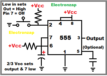
Basic Schmitt Trigger Inverting 555 circuit:
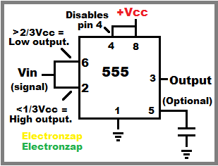
When pins 2 and 6 have the same voltage applied to them, and that voltage gets close to a supply rail voltage, then the output goes as close to the other supply voltage that it can.
A middle ground input voltage (Vin) will leave the output in whatever state it was last put in to. That is the Hysteresis range, and is what makes this circuit a Schmitt Trigger.
Less than 1/3 Vcc applied to pin 2 (Trigger) sets the output high.
More than 2/3 Vcc to pin 6 (Threshold) sets the output low.
Between 1/3 and 2/3 Vcc applied to Pins 2 and 6, leaves the output as it already is.
Practice circuits:
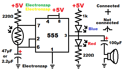
Astable 555 alternating LEDs:
Having 2 LEDs that keep alternating between which one is on and off looks cool.
I also color code the LEDs to help visualize the high versus low output.
I forgot to write Blue and Red, or color in the LED schematic symbols while making this diagram. Of course, any color can be used.
- Blue LED connected between +5V and the 555 output. Lights up when the output is low (connected to ground somewhat well).
- Red LED connected between the 555 output and ground. Lights up when the output is high (Connected to the positive supply, but always with a bit of voltage loss).
Brief 555 Timer Astable Multivibrator Mode Circuit
Blue LEDs need less current than red LEDs to be the same brightness. Plus the 555 output connects internally to ground better than the positive supply. So a higher value resistor is being used to set current through the blue LED than the one setting the current through the red LED.
Reminder for Astable 555 Circuits:
- Output is high while capacitor is charging up to 2/3 supply voltage.
- Pin 7 connects to ground (is low) while output is low, in order to discharge the capacitor until it drops to 1/3 supply voltage in this circuit.
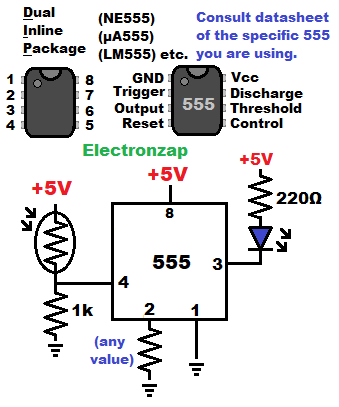
Light Controlled Speaker load plus LED Flasher:
How much light falling on the Light Dependent Resistor (LDR) is the greatest factor that determines output alternating speed in this circuit.
The low value capacitors shown (47µF or 2.2µF) will charge and discharge very quickly when bright light falls on the LED. Bright light drops LDR resistance to somewhat close to 0Ω.
A capacitor makes it so that the current alternates through the speaker with each high and low change of the output. It also stops direct current from flowing through the speaker. Thus limiting wasted power.
I also added LEDs as a visual to this demo circuit.
555 timer and light dependent resistor LDR controlled speaker and alternating LEDs circuit
LED turns on when it is dark 555 circuits:
The goal of both of these circuits is to use a 555 timer to only turn on an LED when it is dark enough.
Low side LDR:
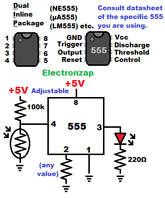
In these circuits, I keep a low input signal applied to pin 2 (trigger). That makes it so that the output will be held high as long as pin down doesn’t get a low input.
A low input to pin 4 (reset), will force the output low. The reset pin over powers the trigger pin when it comes to whether the output is high or low.
The upper circuit gives a high input to pin 4 when is dark. That means pin 2 can make the output high. The LED heads from the output to ground, so it lights up at that time.
When there is a fair amount of light, the upper circuit holds pin 4 low. That sets the output low. Close to zero volts on each side of the LED means it stays off.
High side LDR:
When it is dark, the lower circuit gets a low input to pin 4. That holds the output low. Since the LED heads from the output to the positive supply, the LED lights up due to the voltage difference.
When there is a fair amount of light, the lower diagram circuit gets a high signal to pin 4. That lets pin 2 make the output high. Since the LED connected to the output heads to the positive (high) supply, there is no voltage difference. The LED stays off.
Additional Notes:
You will often see a capacitor across the supply pins. That is to help maintain the voltage across the supply pins, when the supply is unstable. It is a good idea to add one, even if there isn’t one shown in the schematics. I do not add one to most of my videos and schematics because it is distracting to the lesson that I am focused on at the time.
555 limitations:
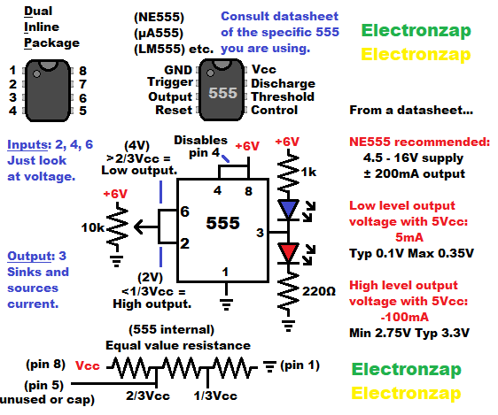
When designing your own circuits, or modifying others, you need to know component limitations. Always consult the datasheet for specific component you have for the most accurate rating. And also remember that lower quality components are common when you buy from less reliable sources. I gathered these numbers from datasheets I found online.
- Absolute Maximum Ratings: Is when you will likely damage the component if you exceed the value given.
- Recommended Operating Conditions: Are what you should aim to stay under as much as possible in order to prolong the life of the component and to reduce the chance of other problems.
Absolute max:
- NE555:
- 18V supply voltage (Vcc).
- Input voltage (control, reset, threshold, trigger) limit is Vcc. In other words, don’t apply a voltage to any of the inputs that exceeds what is powering the 555.
- Inputs just look at the voltage. They don’t pass current, other than a small amount of leakage.
- Output current ±225mA: Don’t sink or source more than 225mA of current.
Recommended operating conditions:
- NE555
- Min 4.5V and Max 16V supply voltage (Vcc).
- Input voltage (control, reset, threshold, trigger) limit is still Vcc. Don’t apply a voltage that exceeds the supply voltage, which is often indicated with “Vcc”.
- Output current of ±200mA: It’s best to sink or source less than 200 milliamps of current.
Possible 555 loads/uses:
- LED(s) turned on and off: Sinking or Sourcing.
- LEDs alternating flashing: Sinking and Sourcing.
- Servo position control by voltage divider.
- Speaker.
- Buzzer.
- Transistor wired as a switch.
- Resetting, or otherwise influencing another 555.
- Bounce free switch.
- Relay with flyback diode.
- Boost converter.
- Interact with all kinds of integrated circuits (ICs).
- Part of amplified microphone circuits.
- Sequential timer.
- Ramp generator.
Related Pages Links:
To support this site, check out the following links:
- Become a Patron!
- Check out my YouTube videos! https://www.youtube.com/c/Electronzap/videos
- Products I used in my videos or otherwise think look like a good buy. As an Amazon associate, I earn from qualifying purchases. https://www.amazon.com/shop/electronzapdotcom
- Information on this site is not guaranteed to be accurate. Always consult the manufacturer info/datasheet of parts you use. Research the proper safety precautions for everything you do.
- Electronzap is a participant in the Amazon Services LLC Associates Program, an affiliate advertising program designed to provide a means for sites to earn advertising fees by advertising and linking to amazon.com.