Table of Contents
Bipolar Junction Transistors (BJTs) are one way to switch a circuit on an off, by means of a weaker electric signal.
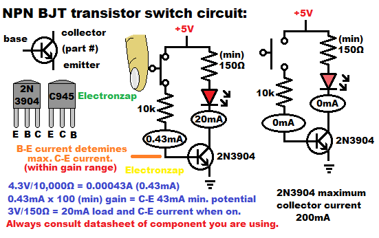
NPN BJT Switch Circuit with push button switch Diagram:
The main take away of this demonstration circuit is that a small base current, allows a much larger amount of collector current. Without base current, there is no collector current, and therefore any load in series with the collector, an LED with protective resistor in this case, will be off.
It’s safe to assume that the 2N3904 NPN BJT has at least 100 gain. Although always check the datasheet for details.
That means that if you want to switch 20mA (0.02A) of current, then you should use at least 0.02A/100 = 0.0002A, or 0.2mA, of current to turn the transistor on fully. The load will set the collector current while the transistor is on. Not the NPN Bipolar Junction Transistor (BJT).
When the push button switch is closed in this circuit, there will be approx. 0.43mA (or 0.00043A) of base current. That is because the base to emitter “diode” drops approx. 0.7V from the base current setting resistor. And 4.3V/10,000Ω = 0.00043A (or 0.43mA) of Base current.
Additional circuit notes:
- Most indicator LEDs have a max. current of 20mA. Red LEDs will probably be plenty bright between 10 and 15mA of current. They will last a lot longer at lower currents. The circuit will behave exactly the same if you use a 220Ω or higher value protective resistor, the LED just won’t be as bright.
- Most BJT switch circuits will have an input from other circuitry controlling it instead of a mechanical switch. Pretty much all mechanical switches can switch an indicator LED by itself, and in a practical circuit, would almost always just switch the LED directly. A mechanical switch is just easier to understand for a simple demonstration circuit than an input signal from other circuitry.
Some 2N3904 NPN BJT specs from a datasheet:
Maximum ratings:
- Collector−Emitter Voltage (VCEO): 40 Vdc
- Collector−Base Voltage (VCBO): 60 Vdc
- Collector Current − Continuous (IC): 200mAdc
- Total Device Dissipation (PD) @ TA = 25°C: 625mW
On characteristics:
- DC current gain (IC = 10 mAdc, VCE = 1.0 Vdc): Min 100: Max. 300:
My notes: The above basically states that you always want to limit Collector current to no more than 200mA, keep the voltage below 40V, keep the transistor total wattage should be kept well below 625mW (0.625W) at approx. room temperature air, and can expect between 100 to 300 gain when 10mA of current is flowing from collector to emitter while 1V is build up across the collector and emitter. There’s a lot more info on the datasheet, but this is some of the most important specs to know for a switch circuit that is properly wired. And as always, I might misinterpret or miswrite something that I am copying. Learn all you can to read datasheets accurately.
Good links to check out next:
To support this site, check out the following links:
- Check out my YouTube videos! https://www.youtube.com/c/Electronzap/videos
- Products I used in my videos or otherwise think look like a good buy. As an Amazon associate, I earn from qualifying purchases. https://www.amazon.com/shop/electronzapdotcom
- Information on this site is not guaranteed to be accurate. Always consult the manufacturer info/datasheet of parts you use. Research the proper safety precautions for everything you do.
- Electronzap is a participant in the Amazon Services LLC Associates Program, an affiliate advertising program designed to provide a means for sites to earn advertising fees by advertising and linking to amazon.com.