Table of Contents
You will learn a lot about electronics while studying bipolar junction transistors (BJTs). Transistor chemistry is primarily what is built into integrated circuits. So, even if you don’t need build a circuit with transistor components, knowing about them will help you understand the limitations of different ICs. There are also many times that you have to add a transistor to an IC base circuit in order to get the desired results.
While building prototype circuits, you will most likely use transistors that are in the TO-92 package. That’s when the plastic transistor component has a curved back side, and a flat front side with the part number on it, and usually some other stuff written on it. Three metal terminals come out of the bottom.
You usually have to find (google search) the datasheet of the part number that you are interested to learn it’s pin layout and other electrical properties specific to that part number. Lots of different types of components come in the TO-92 package. Even 3 terminal integrated circuits.
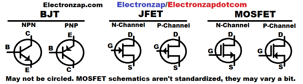
The 2N3904 NPN BJT will work in a lot of circuits that require an NPN BJT. You will often see that part number next to the NPN BJT schematic symbol on a schematic diagram. You can use another NPN BJT that meets the required specification. You just have to make sure that the collector, base, and emitter make the right connections. There’s a number of different pin layouts for BJTs.
NPN versus PNP BJTs and their terminals
BJTs come in 2 flavors:
- NPN
- PNP
And have 3 terminals (metal pins):
- Collector (C)
- Base (B)
- Emitter (E)
Note: The base to emitter junction is basically a diode. That current through it loses about 0.6V to 0.7V. The path from collector to emitter however, does not really drop any noticeable amount of voltage when it is conducting fully (saturated). Just a little, because it isn’t a perfect conductor.
With NPN BJTs, there are 2 current paths. Both currents flow through the emitter, but one of them also flows through the base, and the other also flows through the collector. The current going into the Base and the current going into the Collector combine in the base and exit through the emitter.
Current flows the opposite way through PNP BJTs.
Unfortunately, current (imaginary positive fluid like force flowing from positive to negative) isn’t an accurate portrayal of electricity. It is more accurate to talk about electrons, which flow from negative to positive. The electrons flowing into the NPN emitter, split up and exit through either the base or the collector.
You can build circuits just fine without knowing the exact details of how electrons flow through them. So, this page won’t go into those details. In the future, I may make a page that covers electron flow through BJTs in more detail for those interested in it.
Gain or Beta (ß) or Hfe:
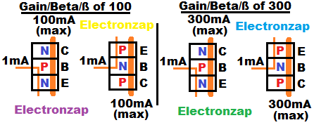
BJTs have the basic electrical property that if you put a little bit of current through the Base, the BJT will let a let more current flow through the collector. Most transistors have a gain that is higher than 100. Generally speaking though, you don’t need to know the exact gain of a transistor. Almost all circuits are designed to work the same as long as the transistor gain meets the minimum required gain.
Instead of Gain, you can refer to it as Beta (ß) or Hfe. They mean the same thing.
- 100 gain means that for every mA of current through the Base, the transistor will let 100mA of current flow through the Collector.
- Gain isn’t set in stone. A particular transistor may have 100 gain in one situation, and 300 gain in another.
Cutoff, Active region, and Saturation:
- Cutoff: No current through the Base, means that the transistor doesn’t allow any current through the Collector. The transistor is off.
- Active region: Some current is going through the Base, which means that current is flowing through the Collector. But. that current is not flowing freely. At least not as much current as the rest of the circuitry will allow.
- Saturation: There is enough Base current that the transistor doesn’t limit the Collector current. Other circuitry limits the Collector current.
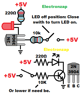
Switch circuit:
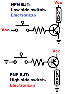
A lot of people wonder why you would use a mechanical switch to control a transistor wired as a switch. It’s likely that you don’t need to. But, it is a good way to practice using a transistor.
While the mechanical switch is open, no current can flow through it. When it is in series with the Base of the BJT, that means that no current can flow through the base. No base current, means that the transistor won’t allow any current to flow the the collector. A load in series with the collector won’t be able to pass any current either. It will be off.
NPN BJT Emitter Follower – Voltage Follower
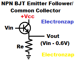
The NPN BJT Base to Emitter drops approx. 0.6V to 0.7V.
A small amount of current from Base to Emitter means that a lot more current will flow from Collector to Emitter.
If there is a load from Emitter to ground, then that means that as soon as the voltage at the Emitter has built up to approx. 0.6V less than the Base voltage, the Base to emitter current will be limited.
A lot more Collector current will flow than Base current, just enough to provide the power demands of the load and maintain the emitter voltage. Therefore a weak signal voltage at the base, should not be thrown off in most cases.
The Emitter voltage will follow any changes in Base voltage by staying 0.6V less.
Some loads may throw off the emitter voltage without a resistor parallel to the load. A parallel resistor helps the emitter get a sense of where 0V ground is. Many circuits may work just fine without the parallel resistor, but it never hurts to include it. 10K is a common value to use for an Emitter to ground resistor.
PNP BJT Emitter Follower – Common Collector – Voltage Follower:
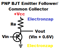
The PNP BJT output is approx. 0.6V higher than the input voltage.
BJT current source:
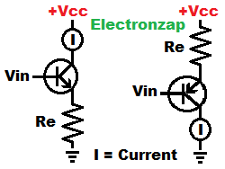
Setting a voltage at the emitter and adding a resistor to ground will set a current based on that voltage an the resistance.
Since that current passes through the collector, that means that it is also the collector current. A load between the supply voltage and collector for NPN, or between collector and ground/negative supply voltage, will also have the same amount of current flowing through it.
Of course there must be enough total supply voltage to power the emitter resistor, collector load, and at least a little voltage that builds up across the transistor.
Cascading NPN and PNP BJTs:
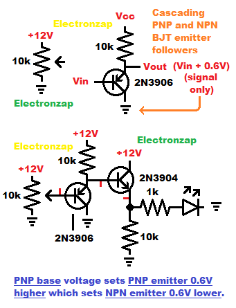
NPN and PNP BJTs emitter followers have opposite offsets.
- NPN Emitter voltage is 0.6V lower than the signal voltage at it’s Base.
- PNP Emitter voltage is 0.6V higher than the signal voltage at it’s Base.
Those voltage are when 0V ground is the negative supply. Some circuits (split/dual) have a supply voltage where there is also a negative voltage in relationship to ground.
Pulses:
Upcoming BJT topics:
There are a lot more topics to add to the this page. I am listing some of them below as I think of them. Many topics deserve their own page, so I will be added them, and linking them, as I update this page.
- Current Source circuit (BJT): NPN vs. PNP:
- BJT specifications (from datasheets).
- Light sensitive circuits, using Light Dependent Resistor (LDR), photodiode, etc.: LDR controlled PNP switch (need to make video).
To support this site, check out the following links:
- Check out my YouTube videos! https://www.youtube.com/c/Electronzap/videos
- Products I used in my videos or otherwise think look like a good buy. As an Amazon associate, I earn from qualifying purchases. My Amazon affiliate page showing products I think look good
- Information on this site is not guaranteed to be accurate. Always consult the manufacturer info/datasheet of parts you use. Research the proper safety precautions for everything you do.
- Electronzap is a participant in the Amazon Services LLC Associates Program, an affiliate advertising program designed to provide a means for sites to earn advertising fees by advertising and linking to amazon.com.