Table of Contents
Bipolar Junction Transistors (BJTs) have a variable amount of current that is allowed to flow from Collector to Emitter. A small amount of Base (to Emitter) current allows many times that amount of current to flow from Collector to Emitter.
It helps to remember these things when looking at a schematic with BJTs.
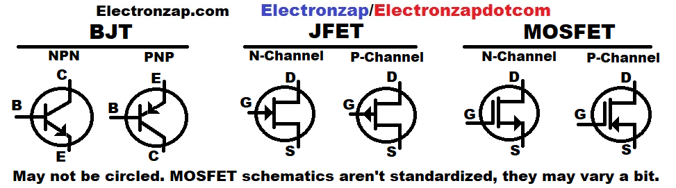
BJTs have 3 terminals:
- Collector (C):
- Base (B):
- Emitter (E):
And come in 2 types of chemistry:
- NPN
- PNP
The BJT symbols shown below are used by almost everyone, although they may not be circled. Whereas, the FET symbols that I use are just 1 of many ways that you will see them if you look at a lot of schematic diagrams. Hopefully there is a part number next to it.
BJT Switch:
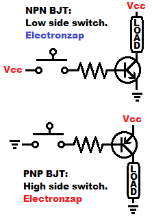
Switch circuits using BJTs are normally off.
- There’s no Collector current without Base current.
- A small amount of Base current allows many times that amount of Collector current. Exact amount depends on the part number of the transistor. Always consult the datasheet.
- BJT switch circuits need to have the transistor conducting freely while it is on. And the BJT needs to not conduct at all while it is off.
- The base to Emitter drops about 0.6V from the resistor used to set the Base to Emitter current.
Without Base current, there will also be no current flow from Collector to Emitter if using NPN BJTs. The Load of a switch circuit is placed on the collector side of the transistor. The load sets the current through it and the collector when the BJT switch is on.
- PNP BJT current flows in the opposite direction of NPN. They are used less often.
The BJT Collector just needs to conduct better than the load in order to be considered fully on. In switch circuits, the load is what limits current.
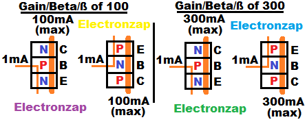
- 100 Gain BJTs need to have the Base pass at least 1% as much current as the load is expected to need. At least 0.2mA Base current if the Collector needs to pass 20mA.
- 300 Gain BJT needs to have the Base pass at least 0.34% as much current as the load is expected to need. At least 0.067mA Base current if the Collector needs to pass 20mA.
- BJTs don’t actually have a set gain. There is a range of gain that it could be based on circuit conditions and individual component variations. Always consult the component’s datasheet and design circuits for the minimum gain that can be expected from the part # you are using.
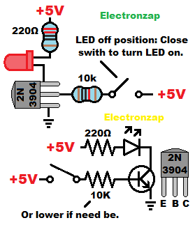
I added a couple example circuits that involve switching an LED on and off with an NPN, and a PNP BJT. In a practical circuit, you would not normally use a mechanical switch to control a BJT switch as mechanical switches do just fine switching by themselves. But, these circuit are an easy introduction to controlling a transistor with 2 voltages (0V= off versus 5V = on), at low currents (through a 10,000 ohm resistor).
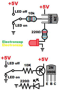
It is good to find simple example circuits like these, and build them on a breadboard to study them. Trying to do so just by looking at a schematic diagram only. Not many pictorials are available to follow.
Keep in mind that different transistor part numbers have a different pin layout and limitations. Always consult the datasheet for that part number to learn the pin layout, and all other important electrical properties.
The NPN 2N3904 and PNP 2N3906 are complimentary pair bipolar junction transistors. They have the same basic limitations, other than passing current in opposite directions.
Light Dependent NPN BJT switch circuit example:
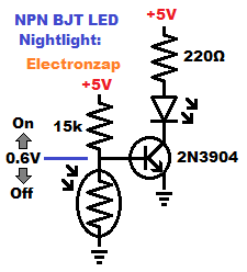
- Under bright light, the low side Light Dependent Resistor (LDR) voltage divider, will set the base voltage of the NPN BJT to close to 0 volts. That keeps the NPN BJT off.
- When it is dark, the low side LDR will have a very high resistance, meaning that positive voltage from the high side fixed resistor will raise the voltage at the base above approx. 0.6V. That will turn the transistor on.
- My YouTube video showing the circuit on a breadboard NPN 2N3904 Bipolar Junction Transistor BJT indicator LED Nightlight circuit schematic diagram
Light Dependent PNP BJT switch circuit example:
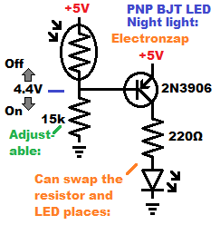
- Bright light falling on the high side LDR voltage makes the LDR conduct well. That holds almost the full positive supply voltage on the PNP BJT base. Making sure that the PNP BJT stays off.
- Without much light on high side LDR, it will provide a lot of resistance. That let the low side fixed pull the voltage closer to ground. Once the voltage is pulled down to less than about 4.4V, the PNP BJT will start turning on.
- My YouTube video showing the circuit on a breadboard PNP 2N3906 Bipolar Junction Transistor BJT indicator LED Nightlight circuit schematic diagram
BJT Emitter Follower/Common Collector:
Bipolar Junction Transistor Emitter Follower circuits, also called Common Collectors, transfer a voltage from a signal to a load. But, with a 0.6V offset.
NPN Follower:
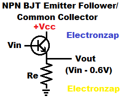
The NPN BJT Emitter follower, has the load on the emitter side of the transistor, indicated by Vout.
It is also a good idea to add a resistor from emitter to ground. Usually a 10k resistor works well
A very small amount of Base current flows through to the emitter, causing a lot more Collector current to also flow through to the emitter.
That collector current builds up a voltage across the load until it is approx. 0.6V less than the signal voltage at the Base. Approx. 0.6V of the signal voltage is built up across the Base and Emitter because it is a diode.
PNP Follower:
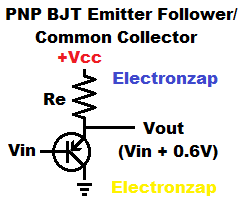
PNP BJT Emitter Followers output a voltage that is 0.6V higher than the signal voltage. But, the current needed to provide that voltage has to flow through the Emitter resistor (Re).
Therefore, the PNP Emitter Follower is usually just used as a signal voltage for other circuitry that is headed to ground.
You can however set a voltage in relation to Vcc, and use the PNP BJT to sink the current to ground.
BJT Current Source:
It’s easy to set a maximum current through a Bipolar Junction Transistor.
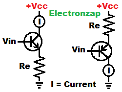
- Voltage across the Emitter resistor (Re) sets the current through the collector. That is as long as a series load doesn’t limit current even more than that.
- Current equals voltage divided by resistance of the emitter resistor: I = V/R
- Voltage at Base transfers to Re, but shifts approx. 0.6V.
- 0.6V less than ground for NPN.
- 0.6V more than ground for PNP. Or, 0.6V less than Vcc.
Related pages:
–-Bipolar Junction Transistor – – –
To support this site, check out the following links:
- Become a Patron!
- Check out my YouTube videos! https://www.youtube.com/c/Electronzap/videos
- Products I used in my videos or otherwise think look like a good buy. As an Amazon associate, I earn from qualifying purchases. https://www.amazon.com/shop/electronzapdotcom
- Information on this site is not guaranteed to be accurate. Always consult the manufacturer info/datasheet of parts you use. Research the proper safety precautions for everything you do.
- Electronzap is a participant in the Amazon Services LLC Associates Program, an affiliate advertising program designed to provide a means for sites to earn advertising fees by advertising and linking to amazon.com.