Table of Contents
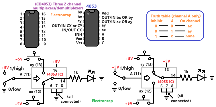
The 4053 has three multiplexer or demultiplexer circuits with 2 channels. A low signal to a control pin of one of the circuits allows only one of the channels to conduct low power or a signal. Whereas a high signal to the control pin allows the other channel to conduct low power or signal. A high (1) input to the inhibit pin stops all channels from conducting. It is generally held low (0).
Note: The schematic SPDT switches that I drew in the 4053 box represent transistors in the IC, not physical switches.

Below is my YouTube channel demonstrating and explaining the diagram above. Please subscribe.
Amazon affiliate link to a kit I have.
Good pages to check out next:
To support this site, check out the following links:
Become a Patron! I currently share my new diagrams with patron supporters and will also share them with anyone that joins my YouTube channel through the following link.
Become a member of my YouTube channel!
- Check out my YouTube videos! https://www.youtube.com/c/Electronzap/videos
- Products I used in my videos or otherwise think look like a good buy. As an Amazon associate, I earn from qualifying purchases. My Amazon affiliate page showing products I think look good
- Information on this site is not guaranteed to be accurate. Always consult the manufacturer info/datasheet of parts you use. Research the proper safety precautions for everything you do.
- Electronzap is a participant in the Amazon Services LLC Associates Program, an affiliate advertising program designed to provide a means for sites to earn advertising fees by advertising and linking to amazon.com.