Table of Contents
MOSFET Drain-Source conduction depends on the voltage at the gate. No current flows through the gate, other than a usually insignificant amount of leakage. There is also small shifting of charges during voltage changes. The gate is very much like a small capacitor.
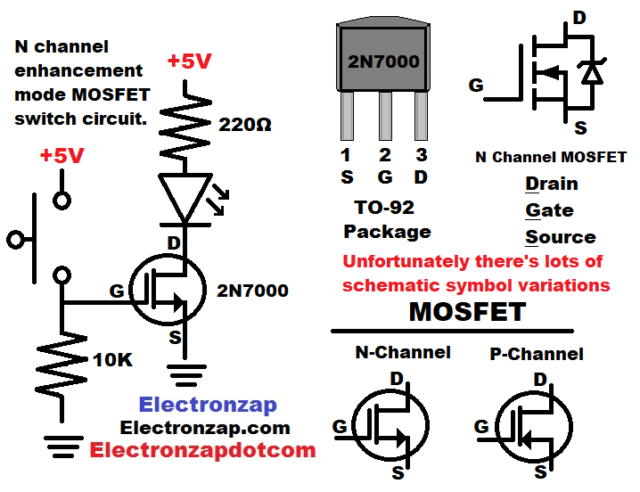
- N channel enhancement mode MOSFET is off (no Drain-Source conduction) when there is a low enough voltage at the gate.
- High enough voltage at the gate turns N channel enhancement mode MOSFET on fully. The Drain-Source conducts as well as the particular transistor can. Always consult the datasheet for specifications of any transistor you are interested in.
Video:
N channel
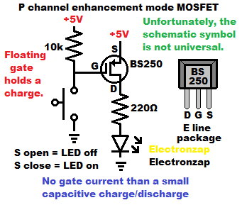
- P channel enhancement mode MOSFET is off (no Source-Drain conduction) when there is a high enough voltage at the gate.
- Low enough voltage at the gate turns P channel enhancement mode MOSFET on fully. The Source-Drain conducts as well as the particular transistor can. Always consult the datasheet for specifications of any transistor you are interested in.
To support this site, check out the following links:
- Become a Patron!
- Check out my YouTube videos! https://www.youtube.com/c/Electronzap/videos
- Products I used in my videos or otherwise think look like a good buy. As an Amazon associate, I earn from qualifying purchases. https://www.amazon.com/shop/electronzapdotcom
- Information on this site is not guaranteed to be accurate. Always consult the manufacturer info/datasheet of parts you use. Research the proper safety precautions for everything you do.
- Electronzap is a participant in the Amazon Services LLC Associates Program, an affiliate advertising program designed to provide a means for sites to earn advertising fees by advertising and linking to amazon.com.