Table of Contents
Bipolar Junction Transistor (BJT) circuits are wired to only power a load when the appropriate signal (some voltage and a very small amount of current) is applied.
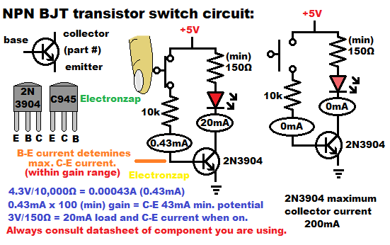
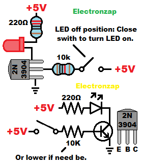
Introduction to NPN BJT switch circuit:
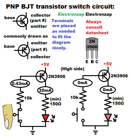
NPN BJTs are placed on the low side of the load due to how current flows through them. PNP BJTs on the other hand are placed on the high side of the load due to how current flows through them. PNP NJT current flows in the opposite direction of NPN BJT current when it comes to their Collector, Base and Emitter terminals.
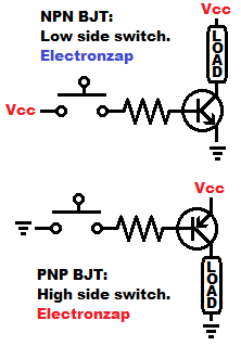
Low side means that the transistor is closer to ground/negative supply than the load. High side means that the transistor is closer to the Vcc/positive supply than the load.
BJT switch circuit properties:
NPN BJTs are studied before PNP BJTs for a number of reasons. The following rules apply to either type of transistor, just keep in mine that PNP current flows in opposite directions.
-
- Load is connected between Collector and the proper voltage supply. Positive for the NPN BJT switch, and negative for the PNP BJT switch. It is in series with the Collector and Emitter as far as the current flowing through them is concerned.
- The load is what limits the current through C-E current in a BJT switch circuit when the transistor is on. When the transistor is off, the BJT is what cuts off current flow through the load.
- Emitter is connected directly to the proper power supply polarity for a witch circuit. Negative/oV/ground for NPN BJTs. Positive/Vcc for PNP BJTs.
- If there is no base current, then there will be no collector to emitter current. Therefore there will be no current through the load.
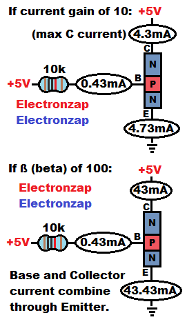
- A small amount of current from B-E (cutoff transistor), allows many times (gain) of current to flow from C-E.
- If C-E is allowed to pass more current then the load. Then the load will be what limits the current based on it’s electrical properties (resistance and/or voltage drop).
- Too little base to emitter current won’t allow the transistor to conduct as much as the load wants. That’s when the transistor is in the active region. The transistor C-E limits current flow in that state, and should be avoided when you want a “switch” circuit. Always make sure to apply enough B-E current to ensure that there is enough C-E current depending on the worst case scenario gain of the BJT you are using.
Always remember that each BJT has a variable gain depending on the voltages across it, and the currents going through it. You just want to make sure that the one you use has more gain than you need.
PNP BJT circuit:
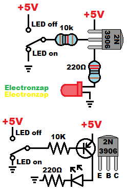
PNP Bipolar junction transistor switches work the same way as NPN (which is usually learned first). With the exception that polarities are opposite. Current of PNP BJTs flows in opposite direction of NPN BJTs, and the transistor is placed closer to the opposite supply voltage in relationship to the load compared to an NPN BJT.
To support this site, check out the following links:
- Become a Patron!
- Check out my YouTube videos! https://www.youtube.com/c/Electronzap/videos
- Products I used in my videos or otherwise think look like a good buy. As an Amazon associate, I earn from qualifying purchases. https://www.amazon.com/shop/electronzapdotcom
This is a new page that will be updated soon!
- Information on this site is not guaranteed to be accurate. Always consult the manufacturer info/datasheet of parts you use. Research the proper safety precautions for everything you do.
- Electronzap is a participant in the Amazon Services LLC Associates Program, an affiliate advertising program designed to provide a means for sites to earn advertising fees by advertising and linking to amazon.com.