Table of Contents
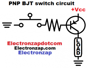
Bipolar Junction Transistors (BJTs) wired as switches use a weak signal (low voltage and/or current) to turn a higher voltage/current load on or off.
PNP BJTs have their emitter connected to the more positive side of the power supply. For the switch circuit, the PNP emitter is directly connected to +Vcc. There can be no components between Emitter and +Vcc when a PNP BJT is wired as a switch.
A small amount of current from emitter to base allows many times more current to flow from emitter to collector.
If a PNP transistor allows over 100 times as much current to flow from emitter to collector as is passing through emitter to base, then it is said to have a gain of over 100.
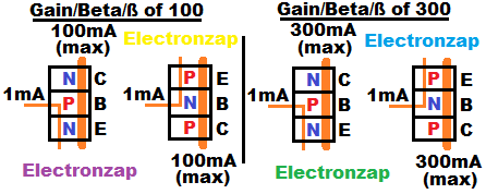
- Most BJTs have a gain over 100. Consult the datasheet of the BJT you are using to learn more about it’s gain.
- The actual gain of a transistor varies a bit by how much current is flowing, and number of other factors.
- Switch circuits need enough base current that the collector will allow more current to flow than what the load sets. In that case, the load is fully on. The BJT is saturated, when it is on.
- No base current, means the transistor is fully off. There can be no collector current when there is no base current.
- Cutoff: When there is no BJT collector current.
Always remember! The load sets the collector current of a BJT switch circuit. There just needs to be enough base current, based on the gain, that the collector doesn’t limit current below what the load will set.
Video:
To support this site, check out the following links:
Really nice looking resistor kit for those beginning studying electronics. Affiliate link ad.
- Become a Patron!
- Check out my YouTube videos! https://www.youtube.com/c/Electronzap/videos
- Products I used in my videos or otherwise think look like a good buy. As an Amazon associate, I earn from qualifying purchases. https://www.amazon.com/shop/electronzapdotcom
- Information on this site is not guaranteed to be accurate. Always consult the manufacturer info/datasheet of parts you use. Research the proper safety precautions for everything you do.
- Electronzap is a participant in the Amazon Services LLC Associates Program, an affiliate advertising program designed to provide a means for sites to earn advertising fees by advertising and linking to amazon.com.