Table of Contents
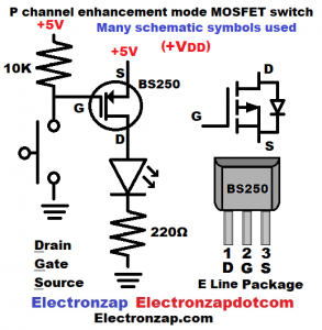
P channel enhancement mode MOSFET has P type material at the Source and also at the Drain. There is an N type material between them.
The gate is close to but separated from the N type material. If you negatively charge the gate, it forces electrons out of the N type material, and it starts acting like a P type material. Thus forming the P channel.
That means that while the gate is negatively charged, electrically speaking, the channel is positively charged. The N type material has electrons removed from it, forming temporary holes that electrons can slip through relatively easily. The enhancement mode transistor conducts current fairly well in that case.
On the other hand, positively charging the gate, just helps put more electrons in the N type material. So there’s solid PNP material, which doesn’t conduct.
Video:
To support this site, check out the following links:
- Become a Patron!
- Check out my YouTube videos! https://www.youtube.com/c/Electronzap/videos
- Products I used in my videos or otherwise think look like a good buy. As an Amazon associate, I earn from qualifying purchases. https://www.amazon.com/shop/electronzapdotcom
This is a new page that will be updated soon!
- Information on this site is not guaranteed to be accurate. Always consult the manufacturer info/datasheet of parts you use. Research the proper safety precautions for everything you do.
- Electronzap is a participant in the Amazon Services LLC Associates Program, an affiliate advertising program designed to provide a means for sites to earn advertising fees by advertising and linking to amazon.com.