Table of Contents
NAND Logic gates need all inputs to be Low in order for the output to be high. That’s the opposite of AND gates, which need all inputs to be high for the output to be high. NAND is a Not AND gate, or inverted AND gate.
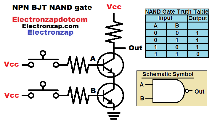
Normally the output is high in this circuit due to the pull up resistor. The switches at the bases of the transistors are normally open. And while they are open, the transistors are off.
But, by closing both switches will apply a high signal to both inputs, results in both transistors connecting the output to ground.
In this circuit, a high output is the positive supply voltage (Vcc), and a low output is 0V ground.
This is just a demonstration circuit. There are integrated circuits (ICs) with NAND gates built in to them if you need one. It is still a good circuit for learning more about electronics.
Nice assortments of semiconductors that I use in my videos. Includes 2N3904 NPN BJTs and 2N3906 PNP BJTs. Amazon affiliate link ad.
Video:
Brief Circuit Schematics with Short Video List of Pages
To support this site, check out the following links:
- Become a Patron!
- Check out my YouTube videos! https://www.youtube.com/c/Electronzap/videos
- Products I used in my videos or otherwise think look like a good buy. As an Amazon associate, I earn from qualifying purchases. https://www.amazon.com/shop/electronzapdotcom
This is a new page that will be updated soon!
- Information on this site is not guaranteed to be accurate. Always consult the manufacturer info/datasheet of parts you use. Research the proper safety precautions for everything you do.
- Electronzap is a participant in the Amazon Services LLC Associates Program, an affiliate advertising program designed to provide a means for sites to earn advertising fees by advertising and linking to amazon.com.