Table of Contents
No current from PNP emitter to base results in there being no emitter to collector current.
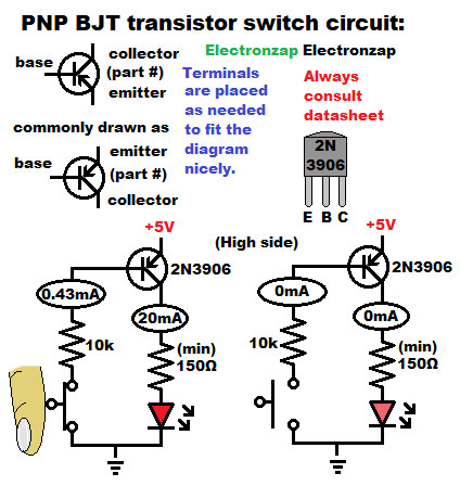
Any load between collector and ground will be off when there’s no base current. There will be no voltage or current flow because it is in series with the emitter to collector.
A small amount of emitter to base current allows a lot of current to flow from emitter to collector. That current also flows through any series load headed from collector to ground. The load is on in that case, and is what limits the current in a switch circuit.
If the load is an indicator LED, then the current needs to be limited to no more than 20mA to protect the LED. A high enough value resistor in series with the LED will be what limits that current, based on the full supply voltage being across the resistor and LED while the transistor is on.
Nice assortments of semiconductors. Amazon affiliate link ad.
The 2N3906 can handle a maximum of 200mA of current from emitter to collector when saturated (conducting fully). In the diagram above, the load will limit the current to 20mA. And then there’s only about 0.43mA of current from emitter to base when the transistor is on. Giving a total of 20.43mA of current through the PNP BJT. The transistor will stay plenty cool.
Red LEDs usually drop about 2V from the protective/current setting resistor. If the supply is 5V, then 5V-2V = 3V will be across the resistor. A 150Ω resistor will set the current to 3V/150Ω = 0.02A, which is usually referred to as 20mA. 3V times 0.02A = 0.06W of power (heat) that the resistor will have to dissipate. Most resistors are rated for 1/4W (0.25W). Therefore it will stay plenty cool in this circuit if exposed to room temperature air.
Note that the collector of the PNP BJT is on the ground (low) side of the circuit compared to the emitter. That means that the load is between the collector and ground. The transistor is on the positive side of the circuit compared to the load. Which is at a higher voltage. Therefore, the switch is on the high side of the load. This is called high side switching.
Video:
To support this site, check out the following links:
- Become a Patron!
- Check out my YouTube videos! https://www.youtube.com/c/Electronzap/videos
- Products I used in my videos or otherwise think look like a good buy. As an Amazon associate, I earn from qualifying purchases. https://www.amazon.com/shop/electronzapdotcom
- Information on this site is not guaranteed to be accurate. Always consult the manufacturer info/datasheet of parts you use. Research the proper safety precautions for everything you do.
- Electronzap is a participant in the Amazon Services LLC Associates Program, an affiliate advertising program designed to provide a means for sites to earn advertising fees by advertising and linking to amazon.com.