Table of Contents
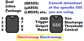
The 555 timer is a well known integrated circuit (IC) that has internal circuitry and terminals (pins) that are used to connect to other external circuitry. It’s primary use is to provide timed high (positive) versus low (negative) power or signals. Timing is usually set by how fast a external capacitor is either charged and/or discharged through external resistance.
Without integrated circuits, Almost every project would require wiring up multiple individual transistors. Some Integrated circuits do the job of billions of transistors even though the IC is very small.
Timing:
Usually a capacitor is used with resistance to set the (monostable/astable modes) timing of the 555 timer output voltage. Capacitors are the symbols that have a couple lines that are separated by a gap. They build up a voltage as current builds up in them. They stop charging or discharging when their voltage is the same as the voltage applied to them.
Capacitors prevent an instant change in voltage (across their terminals), unless they are short circuited. The time it takes for a capacitor to charge and discharge through a resistor is called the RC time constant. Remember that polarized capacitors need to be inserted in the correct direction. Positive side towards positive supply voltage, and negative side towards negative supply voltage.
Output:
The output of the 555 timer (and many other types of ICs) provides either 0V/ground, or somewhat close to the positive supply voltage. 0V is considered being low, whereas close to the positive supply voltage is considered as being high. Most 555 timer outputs drop about 1 to 1.5V of the supply voltage while the output is high. It might be 4V instead of 5V.
The result is that the output is similar to a single pole, double throw switch that can connect to either supply pin of the 555 timer. Within the limitations of the transistors built into the integrated circuit.
The most common types of 555 timers, the NE555 and µA555, can sink or or source a maximum of 200mA of current. Always consult the component’s datasheet to make sure you are staying within the limitation of the component. Keep in mind though that there’s a lot of imitation components out there, that may not be as good as the part # they claim to be.
Bistable mode
Bistable means that the output stays either high, or low, until you force it to change.
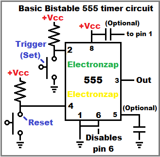
Pins 2 (trigger) and 4 (reset) both have a resistor that holds a high (more positive) voltage on them. That prevents them from changing what the output voltage is.
Pressing the push button switch connected to pin 4 (reset pin) gives a low (0V) voltage to pin 4. Doing so always sets the output low if it isn’t low already, and keeps it low if it is already low. Pin 4 overpowers pin 2. It doesn’t matter if pin 2 is low when pin 4 is set low, the output will be low during that time.
When the push button for pin 2 (trigger) is pressed so that it is connected to ground, setting it low, then the output will be high as long as pin 4 isn’t low. Always remember that a low signal to pin 4 will overpower a low signal to pin 2.
Monostable mode:
A low pulse (quick press of pushbutton switch) to pin 2 (trigger) results in a high output while the capacitor wired to pin 6 (threshold) and pin 7 (discharge) charges through the timing resistor.
Once the capacitor charges to 2/3 of the supply voltage, then pin 3 (output) goes low. As does pin 7, which discharges the capacitor.
Both pins (7 & 3) stay low until forced high again. Low output is the only stable state. Mono means one, therefore it is a monostable circuit. Timing (pin 6 and 7) capacitor value, and resistor value, determine how long it takes the timing capacitor to charge from 0V to 2/3 of the supply voltage.
Astable mode:
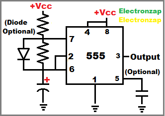
When power is applied, the timing capacitor charges through a resistor and diode in the circuit shown here. Without a diode, the capacitor charges through the 2 resistors.
The output is also high when power is first applied, because pin down sensed that the capacitor was charged to less than 1/3 of the supply voltage.
Once pin 6 (threshold) senses that the capacitor charged to 2/3 of the supply voltage, then the output goes low (connects to ground internally), as does pin 7 (discharge).
During that time, the built up charge in the capacitor discharges through the one resistor and into pin 7. Current also flows from the positive supply (Vcc), through the resistor connected to it, and into pin 7. Vcc to pin 7 current is separate from the capacitor discharge current at this time, so it does not affect the discharge time of the capacitor.
Once the capacitor drops to 1/3 of the supply voltage, then the output goes high again, and pin 7 basically turns off again so that the capacitor can charge.
The process keeps going back and forth as long as power is applies. There is no high or low state that the output will stay in. Astable means that there is no stable state.
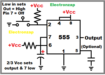
Schmitt Trigger NOT Gate:
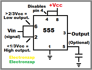
Tying pin 2, pin 6, and a signal voltage together, gives you a Schmitt Trigger NOT gate, or digital inverter circuit.
A low input to pin 2 (trigger) sets the output high, whereas a high input to pin 6 (threshold) sets the output low. Between the 1/3 or less than supply voltage or less low signal, and the 2/3 or more than supply voltage or more signal, there is a middle ground hysteresis area. That’s where the output stays in whichever state it was last put into.
To support this site, check out the following links:
- Check out my YouTube videos! https://www.youtube.com/c/Electronzap/videos
- Products I used in my videos or otherwise think look like a good buy. As an Amazon associate, I earn from qualifying purchases. My Amazon affiliate page showing products I think look good
- Information on this site is not guaranteed to be accurate. Always consult the manufacturer info/datasheet of parts you use. Research the proper safety precautions for everything you do.
- Electronzap is a participant in the Amazon Services LLC Associates Program, an affiliate advertising program designed to provide a means for sites to earn advertising fees by advertising and linking to amazon.com.